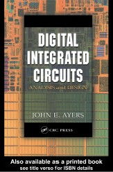
Digital integrated circuits (ICs) are the fundamental building blocks of modern electronics, powering everything from smartphones and computers to complex industrial control systems and data centers. The process of analyzing and designing these circuits is a sophisticated and multi-disciplinary field that combines principles from electrical engineering, computer science, and physics.
1. Core Concepts and Analysis
The journey begins with understanding the core components: transistors, specifically Metal-Oxide-Semiconductor Field-Effect Transistors (MOSFETs). Analysis of digital circuits focuses on modeling the behavior of these transistors in various configurations to form basic logic gates (e.g., NAND, NOR, NOT) and sequential elements (e.g., flip-flops, latches). Key analytical aspects include:
- Static Behavior: Determining the steady-state voltage levels representing logic '0' and '1', and calculating parameters like noise margins, which define the circuit's robustness.
- Dynamic Behavior: Analyzing the transient response, primarily the propagation delay and rise/fall times, which determine the maximum operating speed of the circuit.
- Power Dissipation: Quantifying the power consumed, which consists of dynamic power (due to charging/discharging of capacitances) and static power (due to leakage currents).
- Interconnect Effects: Modeling the impact of wires connecting transistors, including resistance (R), capacitance (C), and inductance (L) effects, which become dominant at advanced technology nodes.
2. The Design Flow
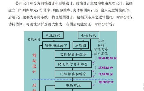
The design of a digital IC is a hierarchical and iterative process, often referred to as the VLSI (Very Large-Scale Integration) design flow.
a. System Specification & Architectural Design:
This initial phase defines the overall functionality, performance targets, power budget, and physical constraints of the chip. High-level architectural decisions, such as the choice of processor core, memory hierarchy, and bus structures, are made.
b. Register-Transfer Level (RTL) Design & Verification:
Designers describe the circuit's behavior using hardware description languages (HDLs) like Verilog or VHDL at the RTL level. This abstract description specifies the flow of data between registers and the operations performed. Extensive functional verification via simulation ensures the RTL code correctly implements the specification.
c. Logic Synthesis & Gate-Level Netlist:
The RTL code is then synthesized into a gate-level netlist—a list of standard cells (pre-designed logic gates) and their interconnections. Synthesis tools optimize the design for area, speed, and power based on constraints provided by the designer.
d. Physical Design (Placement & Routing):
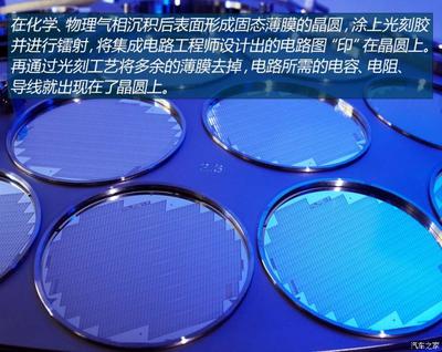
This is the transformation of the logical netlist into a geometric layout. The standard cells are placed on the silicon die, and their interconnections are routed. This stage is critical for meeting timing constraints and minimizing chip area and wire length.
e. Timing Closure & Verification:
After placement and routing, detailed timing analysis (Static Timing Analysis - STA) is performed to verify that all signal paths meet the required clock frequency. This is an iterative process often requiring adjustments to the physical design.
f. Physical Verification & Tape-Out:
The final layout undergoes rigorous checks for design rule violations (DRC), layout versus schematic mismatches (LVS), and electrical rule checks (ERC). Once all checks pass, the design data (GDSII file) is "taped out" to the semiconductor foundry for manufacturing.
3. Challenges and Advanced Topics
The relentless drive for smaller, faster, and more energy-efficient chips, guided by Moore's Law, presents continuous challenges:
- Deep Submicron Effects: At nanometer-scale technologies, effects like process variation, signal integrity issues (crosstalk), and increased leakage power become paramount.
- Design for Testability (DFT): Incorporating structures like scan chains and Built-In Self-Test (BIST) to ensure manufactured chips can be tested for defects.
- Low-Power Design: Employing techniques such as clock gating, power gating, multi-Vt libraries, and dynamic voltage/frequency scaling (DVFS) to manage power consumption.
- System-on-Chip (SoC) Integration: Integrating multiple complex functional blocks (processors, memory, analog interfaces) onto a single die, requiring sophisticated communication architectures and design reuse (IP cores).
Conclusion
The analysis and design of digital integrated circuits is a field defined by constant innovation. It requires a deep understanding of device physics, circuit theory, and computer-aided design (CAD) tools. As technology advances, designers must tackle new physical limitations while architecting systems of ever-greater complexity and capability, making it a challenging yet profoundly impactful engineering discipline.